PFA
Precision Focus Automation
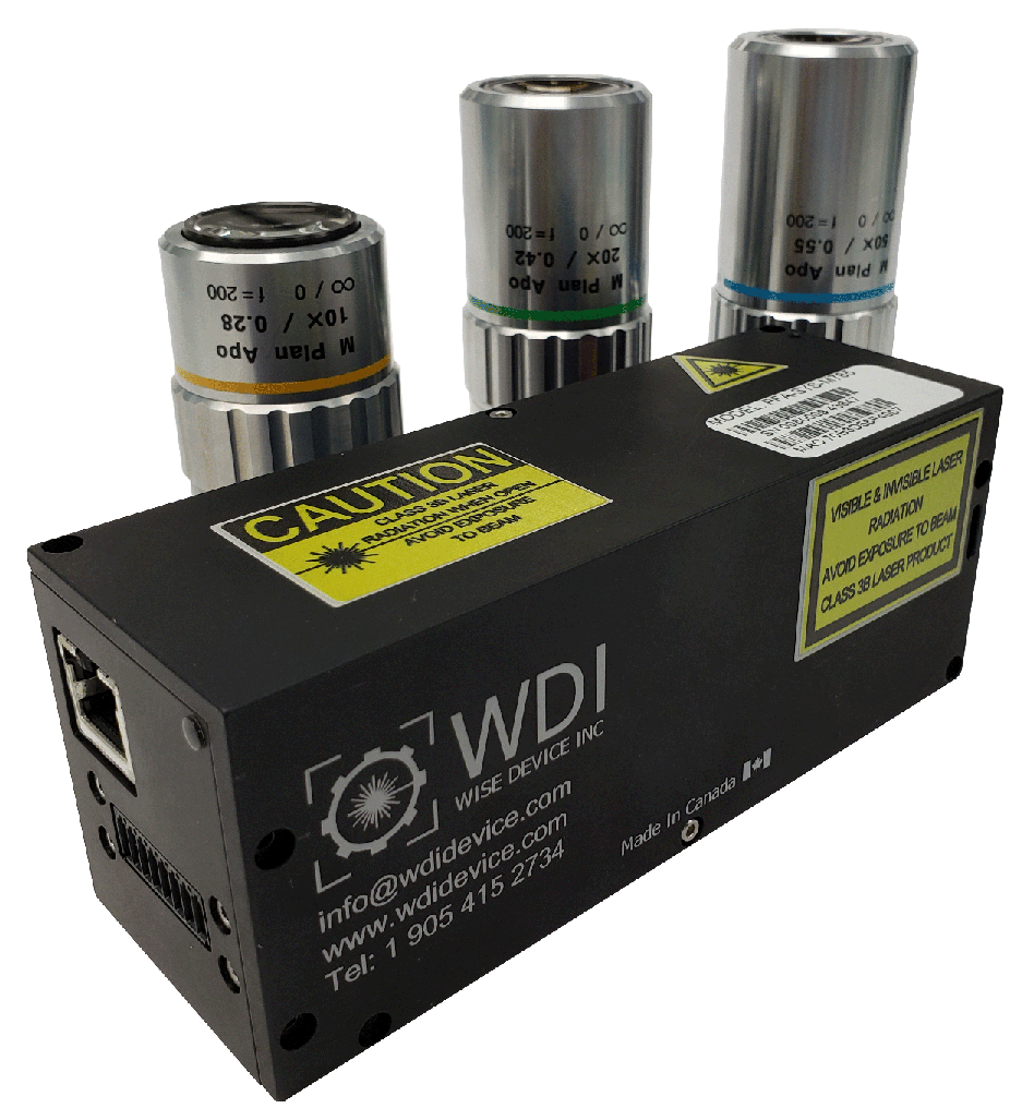
WDI’s next generation Precision Focus Automation “PFA” technology includes the world’s fastest and most powerful microscopy autofocus sensor. Driven by demand for higher speed, greater accuracy and more flexibility for a wider variety of applications the PFA sensor features significant advancements in optics, imaging, processing and communication.
PFA sensors feature:
Higher update rate and faster measurements, greater accuracy and repeatability with improved ease of integration
Fifteen times greater sensitivity, a global shutter and increased speed along with enhanced ability for both laser and video autofocus
Major improvements in memory, processor power and function as well as adaptability and programmability
Gigabit Ethernet communication and Linux OS provide greater reliability and enhanced capabilities
ATF
Auto Focus Sensors
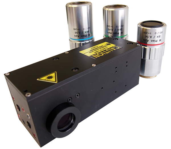
The core of WDI’s technology is our autonomous digital autofocus sensor (ATF) which may be integrated to existing customer supplied or WDI microscope systems. To meet the demands of a wide variety of applications, several sensor models are available, each with its own set of options depending on specific requirements. WDI’s ATF technology is used worldwide in many environments including flat panel display, electronics and semiconductor manufacturing. Our products are also found in biomedical research and imaging automation applications.
All sensors feature:
“Smart Sensor Architecture” (SSA) which incorporates a semiconductor laser, CMOS image sensor, FPGA and microprocessor
High speed, high accuracy, reliable and repeatable performance
The ability to maintains focus on a wide variety of surfaces and substrates that are stationary or moving in real time.
A variety of integration, control and performance options making them adaptable to a wide range of complex applications and demanding environments
PFA MMS
PFA – Modular Microscopy System
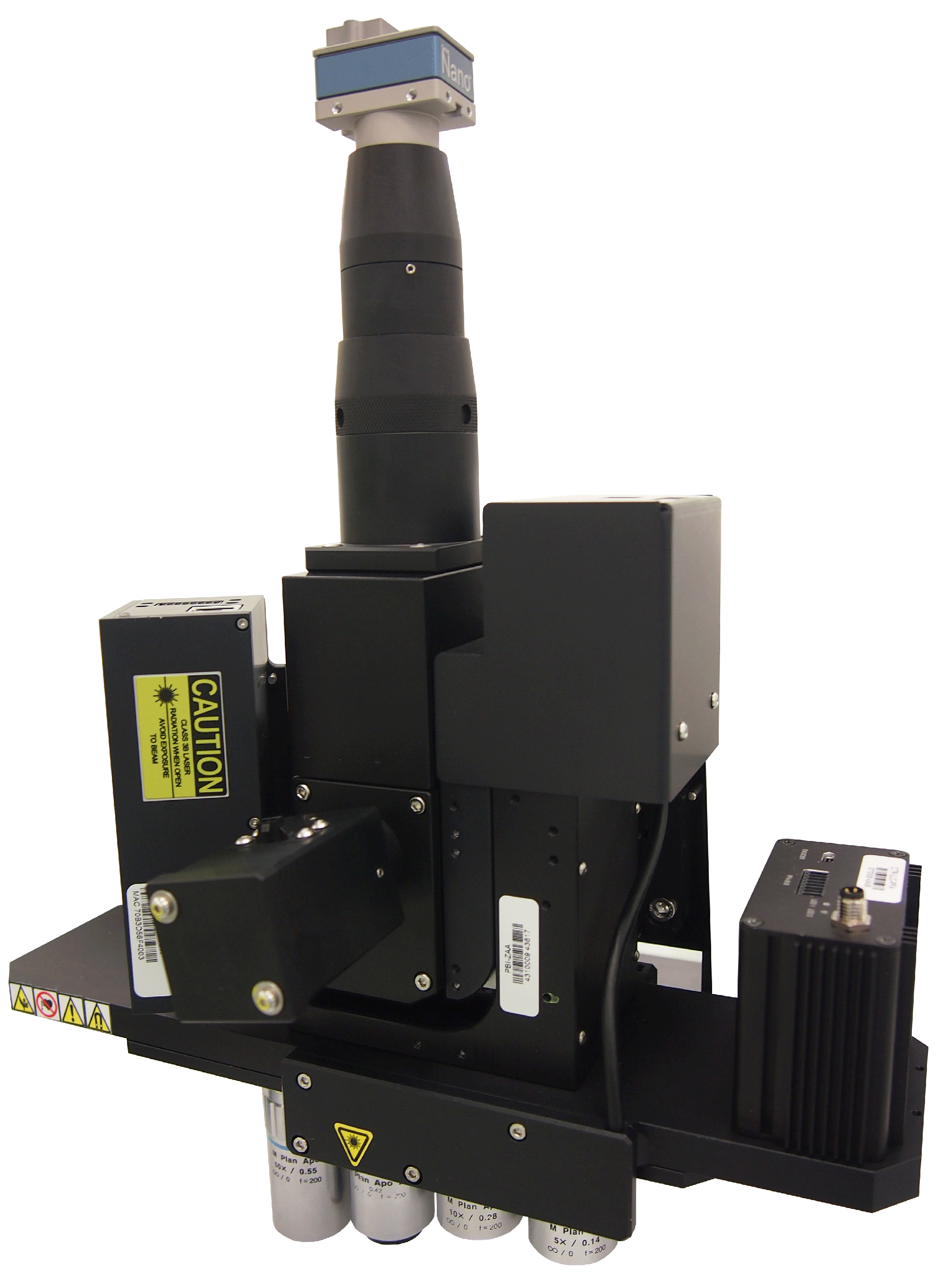
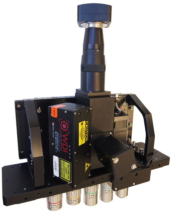
Next generation autofocus and modular microscopy system coupling the world’s fastest most advanced autofocus technology with integrated automation components to create the perfect microscopy system solutions.
All PFA MMS Systems feature:
NEW PFA autofocus sensor with upgraded and improved optics, imaging, processing and communication hardware and capabilities
PFABUS™ communication between components which increases reliability, speed and ease of integration
PFA components including integrated control technology that eliminate external devices and messy cabling
Gigabit Ethernet and a Linux OS providing greater speed and enhanced capabilities
MMS
Modular Microscope Components & Systems
Coupled with our ATF technology WDI designs and manufactures a diverse range of microscopy automation components (MMS) which may be used “stand alone” or part of a complete imaging system. The full line of MMS components include various models of automated linear lens changers, Z-Axis actuators and illuminators as well as microscope bodies, tube lenses and camera mounts.
All MMS products and systems feature:
High performance industrial design adaptable to any application and manufacturing environment.
Precision optical and automation components which are light weight and have a small footprint.
Modularity allowing ease of integration with third party optical components and systems including those from Navitar, Mitutoyo, Excelitas, Olympus, and Nikon
LSCM
Laser Micro Machining Microscopes
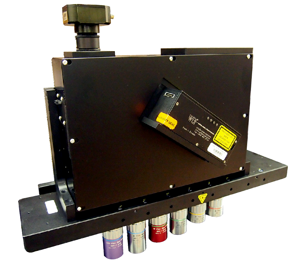
For more demanding industrial microscopy imaging applications and those processes which require a laser for micro machining, trimming or repair WDI has engineered a line automated optical inspection and laser micro machining microscopes (MIC). Like the Modular Microscope System the MIC line easily integrates with WDIs technology to create a fully autonomous system encompassing focus, illumination, and lens actuation.
All MIC systems feature:
Materials and a design suited to meet the demands of modern high speed manufacturing in the LCD, LED, OLED, and semiconductor industries in terms of image quality, system stability, reliability and speed
The capability for both static and high speed scanning applications
The ability to be configured with a laser port and internal optics to allow 2, 3, or 4 laser wavelengths with minimal loss to laser power at the target
IRLC
Infrared Laser Confocal Microscope
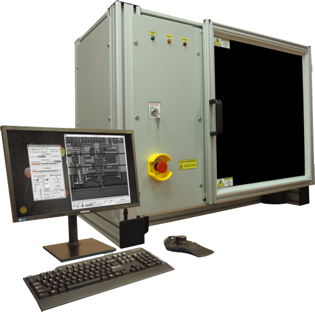
In response to the demands of semiconductor manufacturers for an instrument capable of imaging within a wafer or device in a non-destructive manner, WDI designs and manufactures automated infrared laser confocal microscopes. The IRLC and LSCM allow subsurface and interior inspection of silicon wafers and devices, permitting the imaging of internal structures at sub-micron resolution.
The IRLC features:
Near-IR laser and IR optics coupled with confocal scanning technology ideal for non-destructive subsurface interior investigation of silicon wafers, IC chips, MEMS, Solar Panels, and other devices
A full automation package consisting of a motorized XY stage, objective lens turret, illumination, focus and Z position and laser attenuation
Powerful yet intuitive software, designed to increase the effectiveness and efficiency of the inspection and review processes
Optional automation and recipe software, allowing the system to conduct completely automated inspection routines on individual devices or complete wafers and/or IC strip and tray packages

